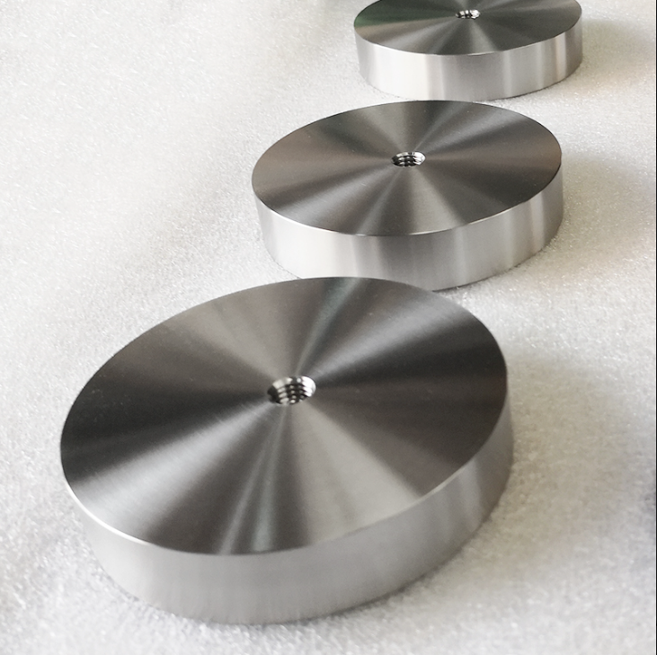
Semiconductor manufacturing demands ultra‑clean, non‑magnetic and corrosion‑resistant materials to avoid wafer contamination and guarantee nanoscale processing accuracy. Titanium and titanium alloys have become critical materials for chip fabrication, covering two core segments: high‑purity titanium sputtering targets for thin‑film deposition, and precision CNC‑machined titanium structural parts for semiconductor equipment.
1. High‑Purity Titanium Sputtering Targets (PVD Thin‑Film)
High‑purity Grade1 / Grade2 titanium (4N ~5N purity) conforming to SEMI standards is widely used for magnetron sputtering. It produces Ti and TiN thin‑films for advanced‑node chips, DRAM and 3D‑NAND.
Adhesion & seed layer: Titanium film improves bonding strength between copper metal layers and silicon‑based dielectric substrates in copper interconnect architecture.
Titanium silicide (TiSi₂): Formed by annealing deposited titanium with silicon. It lowers contact resistance for source, drain and poly‑silicon gates, boosting chip switching speed.
TiN diffusion barrier layer: Titanium nitride thin‑film blocks copper atom diffusion, preventing short‑circuit and device failure. It is essential for copper interconnection.
Metal gate electrode: TiN serves as the metal‑gate material for HKMG / FinFET / GAA advanced processes, replacing traditional poly‑silicon gates.
Note: For high‑aspect‑ratio vias, Ti‑based ALD precursors such as TDMAT are also adopted for conformal TiN deposition.
2. Precision‑Machined Titanium & Titanium Alloy Equipment Parts
Grade2 pure titanium (TA2) and Grade5 titanium alloy TC4 (Ti‑6Al‑4V) are processed into vacuum components for etching, PVD, ion implantation and wet‑cleaning tools.
Grade 2 Pure Titanium (TA2)
Chamber liners, gas distribution rings, vacuum flanges, piping assemblies.
Outstanding resistance to halogen‑based plasma and corrosive wet‑chemistry reagents. Ultra‑low outgassing performance meets UHV (ultra‑high vacuum) requirements and reduces particle contamination on wafers.
Grade5 TC4 Titanium Alloy (Ti‑6Al‑4V)
Wafer robot end‑effectors, handling arms, positioning bases and clamping fixtures.
Core advantage: fully non‑magnetic. Unlike stainless steel, TC4 will not disturb electron‑beam or ion‑beam trajectory. High specific strength and low thermal deformation guarantee micron‑level positioning accuracy for 200 mm / 300 mm silicon wafers.
Wet‑Cleaning Components
TA2 titanium fixtures and tank parts are applied in semiconductor wet cleaning stations, resisting most acid‑base and halogen‑containing chemical solutions.
3. Why Titanium for Semiconductor Manufacturing?
Non‑magnetic property: Critical for e‑beam lithography and ion‑implant equipment.
Ultra‑low outgassing: Suitable for ultra‑high‑vacuum working environment.
Plasma & chemical corrosion resistance: Less particle generation to protect wafers.
Low thermal expansion: Minimum dimensional shift under temperature fluctuation.
High strength‑to‑weight ratio: Light‑weight moving robotic components.
4. Procurement Notes
Sputtering targets: Require high‑purity Grade1 / Grade2 titanium, SEMI‑compliant, strict grain‑size control.
Machine parts: TA2 / TC4 material, precision CNC machining, ultra‑clean surface polishing, CMM dimensional inspection.
If you need custom high‑purity titanium targets or semiconductor‑grade titanium machined components, welcome to contact us for drawings review and quotation.
Technical Guide5 min read·2026-08-05
Titanium Applications in Semiconductor Industry
Learn key titanium applications in the semiconductor industry, including high‑purity titanium sputtering targets and precision‑machined titanium components for etching, PVD, wafer handling and wet‑cleaning processes.